Definition
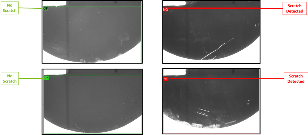
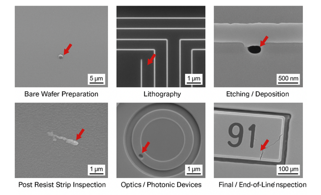
In the semiconductor industry, Automated Optical Inspection (AOI) refers to optical inspection systems used to detect defects, pattern deviations, contamination, and process-induced anomalies on wafers, dies, and advanced packages throughout the manufacturing flow. AOI is deployed at multiple critical steps including front-end wafer processing (lithography, etching, CMP), wafer sort, and back-end processes such as die inspection, advanced packaging, and final assembly. These systems combine high-resolution optics, controlled illumination, precision motion, and advanced image analysis to identify defects at micron and sub-micron scales, enabling early detection of yield loss mechanisms and supporting process control in high-volume manufacturing environments.
General Market Facts
The semiconductor AOI market is driven by continuous device scaling, increasing process complexity, and the diversification of device architectures (logic, memory, power, MEMS, sensors, and heterogeneous integration). AOI systems are now mandatory quality gates in both front-end and back-end manufacturing, complementing metrology and e-beam inspection. While leading-edge fabs invest in extremely high-end inspection tools, a large portion of the market serves mature nodes, specialty devices, and advanced packaging lines, where cost, flexibility, and throughput are critical. Market growth is further fueled by the rise of compound semiconductors, power electronics, and chiplet-based architectures, all of which introduce new inspection challenges not fully addressed by traditional AOI platforms.
Market Segmentation: Application vs. Resolution
AOI systems can be segmented primarily by application and required optical resolution. At the low-resolution end (10–50 µm), AOI is used for macro inspection such as presence/absence checks, packaging inspection, and gross defect detection. Medium-resolution AOI (1–10 µm) addresses metallization inspection, advanced packaging, power devices and micro-assemblies. High-resolution and very high-resolution AOI (<1 µm) target semiconductor wafers, MEMS, micro-optics, and advanced interconnects, often requiring multiple tiled images, precise motion systems, and complex optics. As resolution increases, systems become significantly more expensive and complex, creating a gap in the market for solutions that balance resolution, field of view, throughput, and cost.
Technical Challenges
The core technical challenge in AOI lies in the fundamental trade-off between resolution, field of view, depth of field, and throughput. Achieving sub-micron resolution typically requires high magnification optics with limited field of view and shallow depth of field, leading to increased image count, longer inspection times, and tighter mechanical tolerances. Additional challenges include wafer or part flatness variations, vibration control, illumination uniformity, defect variability, and the need to minimize false positives. On the software side, robust defect detection across process variations remains difficult, especially for low-contrast or stochastic defects. These challenges drive system cost and limit accessibility for many manufacturers.
R2D AOI Project and Value Proposition
R2D’s AOI project aims to address this market gap by developing a modular, scalable inspection platform optimized for high-value applications where conventional AOI systems are either over-specified or cost-prohibitive. The R2D approach combines optimized optical architectures, precise yet cost-effective motion systems, and advanced image processing—including AI-assisted analysis—to maximize usable resolution over large fields of view. The project focuses on flexibility, enabling adaptation to multiple applications (semiconductor, micro-assembly, medical devices) while maintaining industrial robustness and cleanroom compatibility. By targeting the optimal balance between performance, throughput, and cost, R2D positions itself as a differentiated player enabling advanced optical inspection beyond the traditional high-end AOI incumbents.